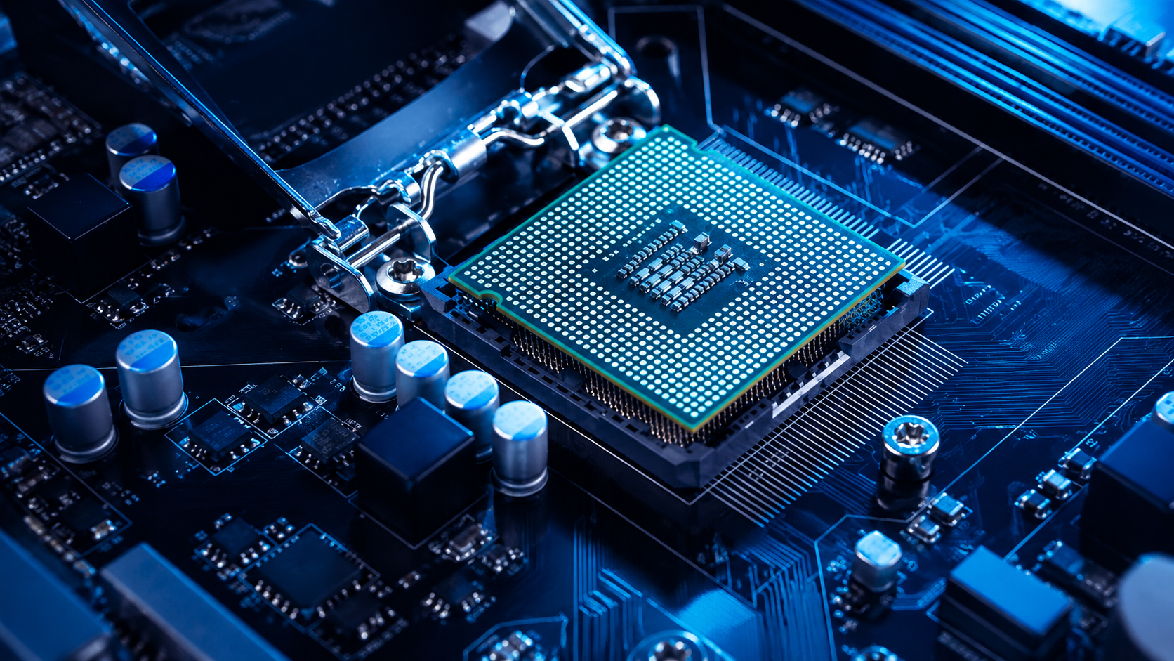
The material and electronic basis of modern computation
A semiconductor is a solid material whose ability to conduct electrical current falls between that of a conductor and an insulator. Its place on this spectrum depends on how easily electrons can move through the material.
Conductors, such as copper, aluminum, and gold, contain a high density of loose electrons that move freely when exposed to an electric field, allowing current to travel through them with minimal resistance. Insulators, such as rubber, glass, and plastic, hold their valence electrons tightly within rigid chemical bonds, creating a high level of resistance that effectively blocks the passage of electrical current.
Semiconductors occupy a highly responsive middle ground. Under baseline conditions at low temperatures, they behave like insulators, keeping their electrons bound. However, when exposed to specific external forces—such as heat, light, or an applied electrical voltage—their atomic bonds loosen, allowing them to conduct electricity.
To avoid confusion, it is helpful to distinguish a semiconductor from nearby technological terms that are often used interchangeably:
- Semiconductor vs. Silicon: Silicon is a specific chemical element (atomic number 14) found abundantly in nature as silica sand. Because of its structural stability and favorable thermal properties, it is the most widely utilized material in commercial electronics. However, it is not the only semiconductor; elements like germanium and compounds like gallium arsenide also function as semiconductors.
- Semiconductor vs. Transistor: A semiconductor is the raw material. A transistor is an engineered device fabricated out of a semiconductor that utilizes its properties to amplify or switch electrical signals.
- Semiconductor vs. Microprocessor: A microprocessor (or microchip) is a complex integrated circuit containing billions of individual transistors, all carved onto a single piece of semiconductor material.
This variable conductivity is best explained by the band theory of solids. Inside any solid material, electrons occupy distinct energy states grouped into bands. The lower energy state where electrons are normally bound to their parent atoms is called the valence band. The higher energy state where electrons are free to move across the material and carry a current is known as the conduction band. The space between these two states is the bandgap, representing an energy zone where electrons cannot stably exist.
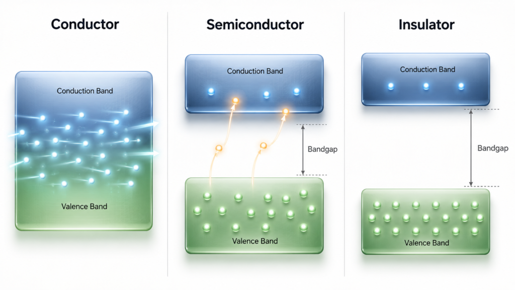
In a conductor, the valence and conduction bands overlap, meaning electrons require no extra energy to move freely. In an insulator, the bandgap is wide, acting as a massive chasm that electrons cannot cross under normal conditions. In a semiconductor, this bandgap is narrow. With a precise addition of external energy, electrons can be pushed across this small gap from the valence band into the conduction band, shifting the material from a resistive state to a conductive one.
Why It Matters
The capacity to alter the electrical state of a material at will is the foundation of digital computation. Before solid-state semiconductors were discovered, early electronic computers relied on vacuum tubes—hollow glass bulbs containing metal electrodes. Vacuum tubes manipulated electricity by burning a filament to release electrons across an empty space toward a receiving plate. This process required significant electrical power, generated substantial heat, and was mechanically fragile. Because vacuum tubes routinely burned out, the scaling potential of early computers was severely limited by physical size and unreliability.
Semiconductors solved this problem by introducing solid-state electronics. Instead of steering electrons across a vacuum, scientists learned to manage electron behavior entirely within solid crystalline structures. This transition offered several profound advantages:
- Extreme Miniaturization: Because solid crystals do not require hot filaments or vacuums, switches could be shrunk from the size of a human thumb to thousands of times thinner than a human hair.
- Unprecedented Energy Efficiency: Solid-state switches require a fraction of the energy needed by vacuum tubes, reducing heat output and allowing millions of switches to operate simultaneously in close proximity.
- Logical Translation: By using an electrical signal to change a semiconductor from an insulating state to a conductive one, engineers can physically represent binary logic. A conductive state represents an open channel (a logical
1), while a resistive state represents a closed channel (a logical0).
Without the responsive properties of semiconductors, the physics of information could not be translated into practical machinery. The entirety of modern computation—from simple calculators to global data networks and advanced artificial intelligence models—rests on our ability to control these microscopic atomic gates.
How It Works
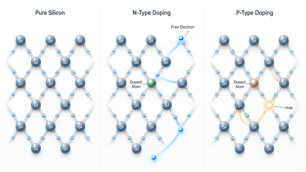
To understand how a semiconductor changes its state, we must look at its crystalline lattice and how it can be modified. Pure silicon serves as the ideal example. A silicon atom possesses four valence electrons in its outermost shell. In a pure, undisturbed crystal—known as an intrinsic semiconductor—each silicon atom shares its four outer electrons with four neighboring atoms through stable covalent bonds.
Because all the valence electrons are locked into this rigid structure, an intrinsic semiconductor lacks the free charge carriers needed to conduct electricity efficiently at room temperature. To unlock its conductive potential, the material must undergo a process called doping. Doping is the intentional introduction of tiny amounts of foreign atoms into the pure crystal lattice to deliberately distort its electrical balance. This creates an extrinsic semiconductor, which can be engineered into two distinct variations:
1. N-Type (Negative) Semiconductors
To create an n-type semiconductor, pure silicon is doped with an element that has five valence electrons, such as phosphorus or arsenic. When a phosphorus atom replaces a silicon atom within the lattice, four of its electrons form covalent bonds with the surrounding silicon. The fifth electron is left without a partner, bound loosely to its nucleus. With a minor amount of thermal or electrical energy, this extra electron escapes into the conduction band, becoming a mobile, negatively charged carrier that can move freely through the crystal.
2. P-Type (Positive) Semiconductors
To create a p-type semiconductor, pure silicon is doped with an element containing only three valence electrons, such as boron or gallium. When a boron atom integrates into the silicon lattice, it can only form three covalent bonds, leaving a vacancy where a fourth bond should be. This structural vacancy is called a hole. While a hole is simply the absence of an electron, it behaves like a mobile positive charge. If an electron from an adjacent silicon atom moves to fill the hole, it creates a new vacancy behind it. In this manner, holes move through the material, acting as positive charge carriers.
The P-N Junction
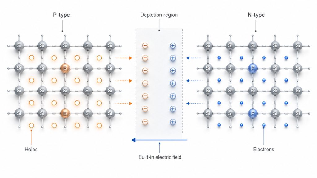
The core mechanism of modern electronics emerges when an n-type material and a p-type material are joined together, forming a p-n junction.
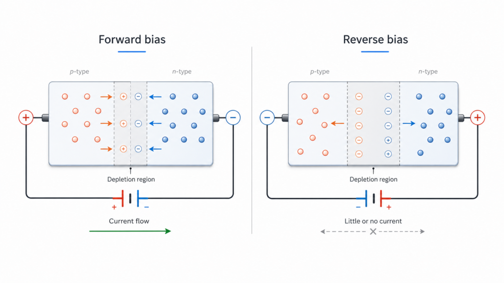
At the exact boundary where these two regions meet, a spontaneous reaction occurs. Free electrons from the n-side migrate across the border to fill the vacant holes on the p-side. This local recombination forms a narrow boundary zone called the depletion region, so named because it is depleted of mobile charge carriers.
As electrons leave the n-side, they leave behind positively charged donor ions. Meanwhile, the electrons entering the p-side create a line of negatively charged acceptor ions. This separation of charges creates a localized, internal electric field across the junction. Eventually, this field grows strong enough to halt further electron migration, establishing a state of equilibrium.
The structural behavior of the p-n junction can be altered by applying an external voltage, a technique known as biasing:
- Reverse Bias: If you connect the positive terminal of an external power source to the n-side and the negative terminal to the p-side, the external field pulls free electrons and holes away from the center boundary. This action widens the depletion region, preventing current from crossing the junction. The material acts as an insulator.
- Forward Bias: If you reverse the connections—attaching the positive terminal to the p-side and the negative terminal to the n-side—the external voltage overcomes the internal electric field, pushing electrons and holes toward the center line. The depletion region narrows and collapses, allowing electrical current to flow across the boundary with ease. The material acts as a conductor.
By acting as a one-way valve for electricity, the single p-n junction functions as a diode.
The Transistor Architecture
By combining multiple doped layers, engineers construct the Metal-Oxide-Semiconductor Field-Effect Transistor (MOSFET), the fundamental switch found inside computer processors.
In a typical n-channel MOSFET, a p-type substrate contains two separate islands of highly doped n-type material. One island is called the source and the other is the drain. Electrical current wants to travel from the source to the drain, but it is blocked by the p-type material sitting between them, which forms two back-to-back p-n junctions.
To open the pathway, a third terminal called the gate is positioned directly above this central p-type channel. The gate is separated from the semiconductor material by an ultra-thin insulating layer of silicon dioxide. When a positive voltage is applied to the gate, it generates an electric field that passes through the insulation. This field repels the positive holes in the central channel and attracts free electrons up to the surface, creating a temporary bridge of electrons between the source and the drain. This temporary bridge is called an inversion layer or channel.
- When voltage is applied to the gate, the channel opens, current flows, and the transistor registers a 1.
- When the gate voltage is turned off, the channel collapses, current stops, and the transistor registers a 0.
By cycling this gate voltage on and off billions of times per second, the transistor functions as a high-speed switch, allowing physical material properties to execute logical code.
History
The evolution of semiconductor physics progressed from a series of strange laboratory anomalies into a highly structured manufacturing paradigm that reshaped human infrastructure.
- 1833: The Temperature Anomaly: Michael Faraday discovers that the electrical conductivity of silver sulfide increases when it is heated. This behavior directly contradicted that of typical metals, whose conductivity decreases as temperatures rise, providing one of the earliest recorded glimpses of semiconductor physics.
- 1874: Discovery of Rectification: German physicist Ferdinand Braun observes that current flows in only one direction when a pointed metal wire is placed in contact with a galena crystal. This discovery led to the development of “cat’s-whisker” crystal detectors, which allowed early radios to receive wireless signals.
- 1947: The Solid-State Breakthrough: Working at Bell Labs, John Bardeen, Walter Brattain, and William Shockley invent the point-contact transistor using the semiconductor element germanium. By demonstrating that a solid crystal could amplify electrical signals without a vacuum, they created an alternative to the vacuum tube and received the 1956 Nobel Prize in Physics.
- 1958–1959: The Integrated Circuit: Jack Kilby of Texas Instruments and Robert Noyce of Fairchild Semiconductor independently develop methods to manufacture multiple components on a single substrate. Instead of assembling circuits from discrete pieces of wired hardware, they realized that transistors, diodes, and resistors could be etched directly onto a single slice of semiconductor material, vastly reducing system complexity and footprint.
- 1965: The Scaling Roadmap: Gordon Moore, an engineer and co-founder of Intel, observes that the number of transistors on an integrated circuit doubles roughly every two years while costs drop. This empirical projection, known as Moore’s Law, became a driving roadmap for the global technology industry, guiding decades of engineering progress and manufacturing investment.
After Moore’s observation, the industry’s progress became visible in the steady compression of the manufacturing process itself. In 1968, advanced chips were produced at roughly 20 micrometers. By 2025, leading-edge fabrication had moved toward 2 nanometers. This long descent from micrometers to nanometers represents the physical side of semiconductor scaling: each new process generation allowed smaller transistor features, denser circuits, faster switching, and lower power use.
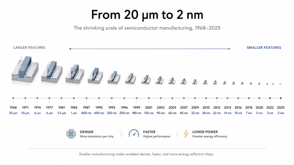
By the time semiconductor nodes reached the nanometer scale, the easy version of scaling had begun to break down. Smaller transistors were still possible, but they no longer delivered the effortless gains that defined the early Moore era. Heat, leakage, manufacturing cost, and atomic-scale precision made every new generation harder.
So Moore’s Law did not simply end. It changed shape. The future of chips now depends not only on shrinking transistors, but on redesigning transistor structures, stacking components vertically, moving power delivery, and packaging many specialized chiplets into a single system.
The old question was: how small can we make the transistor? The new question is: how much computation can we build per unit of silicon, energy, and cost?
In Context
Semiconductors are materials whose electrical properties make modern computation possible. They are not isolated components; instead, they serve as the physical foundation for the broader network of modern technology, linking material physics to large-scale global infrastructure.
| Related Concept | Relationship Type | Conceptual Connection |
| Electricity | Depends on | Semiconductors rely directly on the physical movement of electric charge to alter their internal conductivity states and process computational logic. |
| Information | Enables | By shifting predictably between conductive and resistive states, semiconductors give physical form to the abstract 0s and 1s needed to store, manipulate, and transfer data. |
| Neural Networks | Component of | Artificial learning algorithms operate by running trillions of mathematical vector calculations across physical hardware made entirely of semiconductors. |
| Transformer | Enables | The intensive attention mechanisms used in modern AI architectures require dense, highly integrated parallel processing engines that depend on advanced semiconductor designs. |
| Large Language Models | Sustains | Generative language models utilize billions of statistical parameters that must be calculated and sustained across vast clusters of semiconductor processing hardware. |
| Data Centers | Component of | Data centers are the physical facilities constructed to aggregate, power, cool, and network millions of semiconductor chips working in parallel. |
| Power Grid | Constrained by | Advanced semiconductor fabrication plants (fabs) and modern operational data centers require continuous, highly stable power delivery, placing intense demands on local grid reliability. |
The densest technical areas are the sections on band theory, doping, p-n junctions, MOSFET architecture, and the future limits of transistor scaling.
The Next Frontier
As individual transistors are shrunk down to physical scales measured in single-digit nanometers—the width of a few dozen silicon atoms—they encounter fundamental barriers imposed by quantum physics. At these atomic dimensions, the insulating layers separating the gate from the channel become so thin that a phenomenon known as quantum tunneling occurs. Electrons begin to spontaneously pass straight through the insulating barriers even when the transistor is turned off. This creates continuous electrical leakage, resulting in wasted power and severe thermal buildup that threatens to halt the historical trajectory of Moore’s Law.
To move past these boundaries, researchers are looking beyond silicon toward alternative materials and novel physical designs. One major area of advancement is the deployment of wide-bandgap semiconductors, such as Gallium Nitride (GaN) and Silicon Carbide (SiC). Because these materials feature a significantly larger bandgap than standard silicon, they can withstand far higher voltages, temperatures, and frequencies without breaking down. This makes them ideal for the power electronics found in electric vehicle drivetrains, telecommunications hardware, and renewable energy systems, where managing power density is critical.
For high-performance computation, researchers are developing two-dimensional (2D) materials, such as graphene and transition metal dichalcogenides (like molybdenum disulfide). These materials consist of sheets that are just a single atom thick. By confining electron movement to a two-dimensional plane, engineers can achieve unparalleled control over the electrical current, preventing quantum leakage even at atomic scales. When paired with advanced packaging strategies—such as stacking processing layers vertically in 3D structures and dividing large processors into specialized “chiplets”—the semiconductor industry is shifting its focus from simple size reduction toward advanced material orchestration.
Leave a Reply